2D nanomaterials, with a thickness of a single layer of atoms, have unique electrical and optical properties that make them good candidates for use in electronics and optical sensors. An increasing range of these ultrathin materials can now be synthesized, and the ways in which they emit and absorb light can change based on their structures and positions.
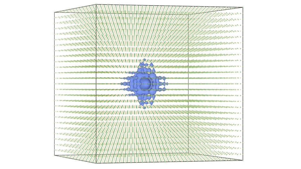
Now, scientists have used the Summit supercomputer at the Oak Ridge Leadership Computing Facility (OLCF) and the Theta supercomputer at the Argonne Leadership Computing Facility (ALCF) to more accurately simulate the optical properties of a 2D nanomaterial called germanium selenide (GeSe) and discovered that the properties of a single layer of GeSe are extremely dependent on the way its atoms are arranged. The team employed a new method that allowed the team members to model geometries of different GeSe structures.
“The ability to use new techniques to model this material on Theta and Summit allowed us to largely avoid the shortcuts and approximations used in earlier methods,” said Paul Kent, computational nanoscience researcher at the US Department of Energy’s (DOE’s) Oak Ridge National Laboratory (ORNL) and director of the Center for Predictive Simulation of Functional Materials. The team’s results were published in Physical Review Materials.
Attractive for applications such as solar cells and photodetectors—devices used to identify the presence of light—GeSe has been of interest in the applied physics community for some time.
Understanding the properties of new and forthcoming materials such as GeSe can help scientists determine which ones warrant a deeper look.
The team plans to study other materials in the same family of elements, applying the method to materials whose geometries are still unknown.
Illuminating tunable materials
When scientists want to model a 2D material, they must predict the lowest energy, or most stable, structure. Typically, forces on an initial structure are computed and the atoms gradually moved to find the smallest net forces and lowest energies. However, the team applied an alternative algorithm that let team members bypass calculating forces and allowed them to use quantum Monte Carlo (QMC) methods.
QMC methods are highly accurate techniques used to study the energies of complex quantum systems. Team member Jaron Krogel at ORNL recently developed the new algorithm for the GeSe structures in an effort that will shortly be the subject of a dedicated publication. Although forces are computationally expensive to obtain in QMC, the new algorithm allows for the use of an optimal combination of more economical methods, saving supercomputer time.
“Running the new structural optimization algorithm within QMC on ALCF and OLCF systems enabled us to accurately determine the geometry of a complex 2D nanomaterial for the first time,” said Hyeondeok Shin, physicist and computational scientist at DOE’s Argonne National Laboratory.
Scientists can change how materials such as GeSe emit and absorb light by pulling, pushing, or twisting their geometries. These materials have tunable electronic bandgaps, which determine the minimum energy and therefore color of any photon that can be emitted or absorbed.
After earning computing time through the Innovative and Novel Computational Impact on Theory and Experiment (INCITE) program, Shin used Theta, Summit, and QMCPACK, an electronic structure code for QMC algorithms, to accurately estimate the bandgap energies for different geometric arrangements of GeSe.
“As a monolayer, GeSe is a wide-bandgap semiconductor that can be engineered for various technical applications,” Shin said. Monolayered materials comprise only one layer of atoms. “These simulations will help us determine whether we could expand its applications to things like field-effect transistors—which use electric fields to control the flow of electrical current—or even LEDs.”
Unlocking new element combinations
Because QMC is computationally expensive, the team’s simulations required the power of DOE’s leadership-class supercomputers. The team first performed approximately 77 separate simulations of 720-electron GeSe systems to optimize five different geometrical parameters on the ALCF’s Theta supercomputer. For the team’s bandgap simulations, the team used the OLCF’s IBM AC922 Summit, the nation’s most powerful and smartest supercomputer, to model systems of up to 1,080 electrons for the bandgap estimates. The OLCF and ALCF are DOE Office of Science user facilities located at ORNL and Argonne, respectively.
Kent added that simulations on Summit allow the team to make more confident predictions or look at more complex materials made of elements from a wider range of the periodic table of elements.
The team hopes to simulate more complex materials in the future that might have applications in photodetectors, gas sensors, and anode materials for lithium-ion batteries.
Related Publication: Hyeondeok Shin, Jaron T. Krogel, Kevin Gasperich, Paul R. C. Kent, Anouar Benali, and Olle Heinonen, “Optimized Structure and Electronic Band Gap of Monolayer GeSe from Quantum Monte Carlo Methods,” Physical Review Materials 5, no. 2 (2021): 024002, doi:10.1103/PhysRevMaterials.5.024002.
This article was originally published on the OLCF website.
==========
The research was supported by DOE’s Office of Science. UT-Battelle LLC manages Oak Ridge National Laboratory for DOE’s Office of Science, the single largest supporter of basic research in the physical sciences in the United States. DOE’s Office of Science is working to address some of the most pressing challenges of our time. For more information, visit https://energy.gov/science.
Argonne National Laboratory seeks solutions to pressing national problems in science and technology. The nation’s first national laboratory, Argonne conducts leading-edge basic and applied scientific research in virtually every scientific discipline. Argonne researchers work closely with researchers from hundreds of companies, universities, and federal, state and municipal agencies to help them solve their specific problems, advance America’s scientific leadership and prepare the nation for a better future. With employees from more than 60 nations, Argonne is managed by UChicago Argonne, LLC for the U.S. Department of Energy’s Office of Science.
The Argonne Leadership Computing Facility provides supercomputing capabilities to the scientific and engineering community to advance fundamental discovery and understanding in a broad range of disciplines. Supported by the U.S. Department of Energy’s (DOE’s) Office of Science, Advanced Scientific Computing Research (ASCR) program, the ALCF is one of two DOE Leadership Computing Facilities in the nation dedicated to open science.
The U.S. Department of Energy’s Office of Science is the single largest supporter of basic research in the physical sciences in the United States and is working to address some of the most pressing challenges of our time. For more information, visit https://energy.gov/science.