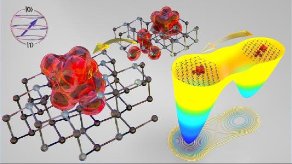
“A totally unexpected and exciting finding was that divacancies can convert into an entirely new type of defect,” added Lee. These newly discovered defects consist of two carbon vacancies paired with what scientists call an anti-site. That is a site in which a carbon atom has filled the vacancy left open by the removal of a silicon atom.
A first of its kind, the team’s simulations were made possible by the development of new simulation algorithms and the coupling of computer codes developed by the DOE-funded Midwest Integrated Center for Computational Materials (MICCoM), headquartered at Argonne and led by Galli. Juan de Pablo a senior scientist in the Materials Science Division and UChicago professor of molecular engineering, developed the new algorithms, which are based on concepts from machine learning, a form of artificial intelligence.
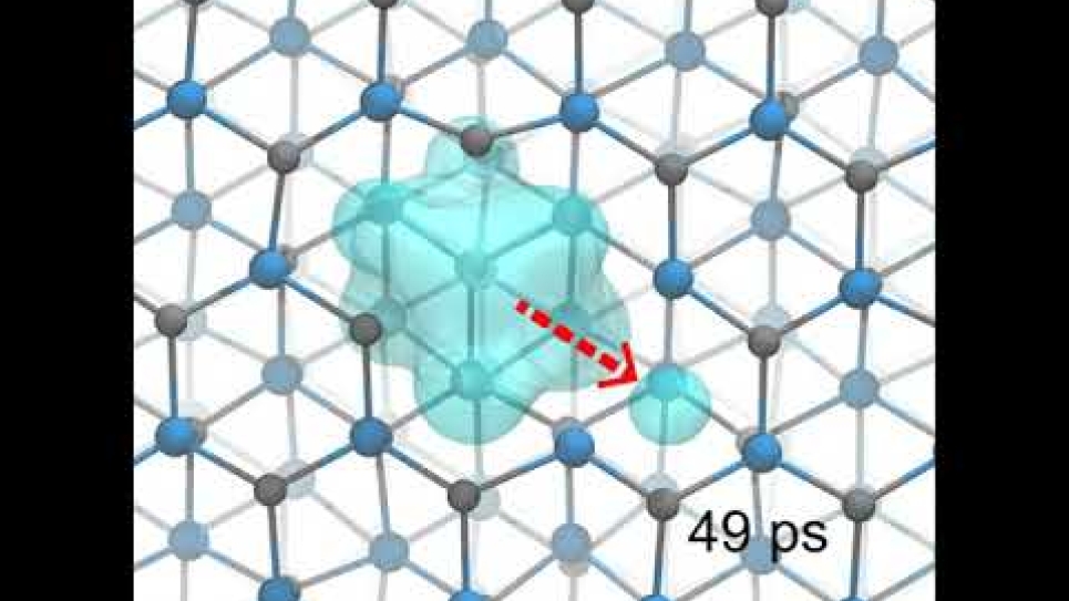
“The formation and the motion of vacancies or defects in semiconductors are what we call rare events,” said de Pablo. “Such events happen on time scales much too long to study in conventional molecular simulations, even on the fastest computer on the planet. It is critical that we develop new ways of promoting the occurrence of these events without altering the underlying physics. That’s what our algorithms do; they make the impossible possible.”
Lee coupled the various codes, building on the work of MICCoM scientists Galli and de Pablo. Over the years, several other scientists were also involved in code coupling, including Francois Gygi at the University of California, Davis, and Jonathan Whitmer at Notre Dame University. The outcome is an important and powerful new toolset combining quantum theory and simulations for investigating vacancy formation and behavior. This will be applicable to not only silicon carbide, but other promising quantum materials.
“We are just at the beginning,” said Galli. “We want to be able to do our computations much faster, simulate many more defects and determine what the best defects are for different applications.”
The team’s paper, “Stability and molecular pathways to the formation of spin defects in silicon carbide,” appeared in Nature Communications. Also contributing was postdoctoral fellow Alvin Yu, University of Chicago. This work was supported by the DOE Office of Basic Energy Sciences. The computationally intense simulations used several high-performance computing resources: Bebop in Argonne’s Laboratory Computing Resource Center; the Argonne Leadership Computing Facility (ALCF), a DOE Office of Science user facility; and the University of Chicago’s Research Computing Center. The team was awarded access to ALCF computing resources through DOE’s Innovative and Novel Computational Impact on Theory and Experiment, or INCITE, program.
==========
Argonne National Laboratory seeks solutions to pressing national problems in science and technology. The nation’s first national laboratory, Argonne conducts leading-edge basic and applied scientific research in virtually every scientific discipline. Argonne researchers work closely with researchers from hundreds of companies, universities, and federal, state and municipal agencies to help them solve their specific problems, advance America’s scientific leadership and prepare the nation for a better future. With employees from more than 60 nations, Argonne is managed by UChicago Argonne, LLC for the U.S. Department of Energy’s Office of Science.
The U.S. Department of Energy’s Office of Science is the single largest supporter of basic research in the physical sciences in the United States and is working to address some of the most pressing challenges of our time. For more information, visit https://energy.gov/science.
The Argonne Leadership Computing Facility provides supercomputing capabilities to the scientific and engineering community to advance fundamental discovery and understanding in a broad range of disciplines. Supported by the U.S. Department of Energy’s (DOE’s) Office of Science, Advanced Scientific Computing Research (ASCR) program, the ALCF is one of two DOE Leadership Computing Facilities in the nation dedicated to open science.
About the Advanced Photon Source
The U. S. Department of Energy Office of Science’s Advanced Photon Source (APS) at Argonne National Laboratory is one of the world’s most productive X-ray light source facilities. The APS provides high-brightness X-ray beams to a diverse community of researchers in materials science, chemistry, condensed matter physics, the life and environmental sciences, and applied research. These X-rays are ideally suited for explorations of materials and biological structures; elemental distribution; chemical, magnetic, electronic states; and a wide range of technologically important engineering systems from batteries to fuel injector sprays, all of which are the foundations of our nation’s economic, technological, and physical well-being. Each year, more than 5,000 researchers use the APS to produce over 2,000 publications detailing impactful discoveries, and solve more vital biological protein structures than users of any other X-ray light source research facility. APS scientists and engineers innovate technology that is at the heart of advancing accelerator and light-source operations. This includes the insertion devices that produce extreme-brightness X-rays prized by researchers, lenses that focus the X-rays down to a few nanometers, instrumentation that maximizes the way the X-rays interact with samples being studied, and software that gathers and manages the massive quantity of data resulting from discovery research at the APS.